Difference between revisions of "Application Note: MM002 Hardware Overview"
(→Pins assignment) |
(→Using with companion MCU chipset) |
||
| (2 intermediate revisions by the same user not shown) | |||
| Line 139: | Line 139: | ||
Optional pin to connect to companion MCU is RESET (module pin 2). Reset is active at low level. | Optional pin to connect to companion MCU is RESET (module pin 2). Reset is active at low level. | ||
| − | It is recommended to add a 100nF capacitor on Reset pin: this will avoid any | + | It is recommended to add a 100nF capacitor on Reset pin: this will avoid any untimely reset of the product due to ESD discharges. |
The others I/O pins can be left not connected. | The others I/O pins can be left not connected. | ||
| Line 193: | Line 193: | ||
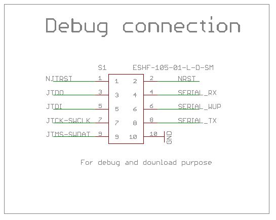
== Schematic == | == Schematic == | ||
| − | [[File: | + | [[File:schéma lora.JPG]] |
[[File:Power supply.JPG]] | [[File:Power supply.JPG]] | ||
| Line 201: | Line 201: | ||
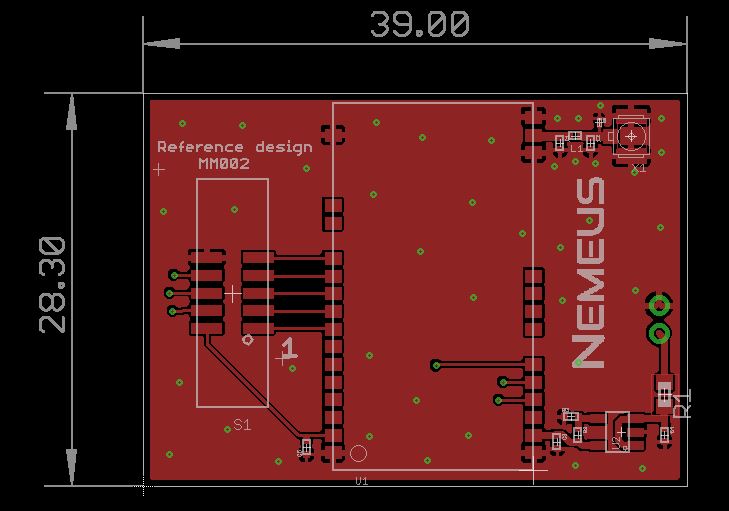
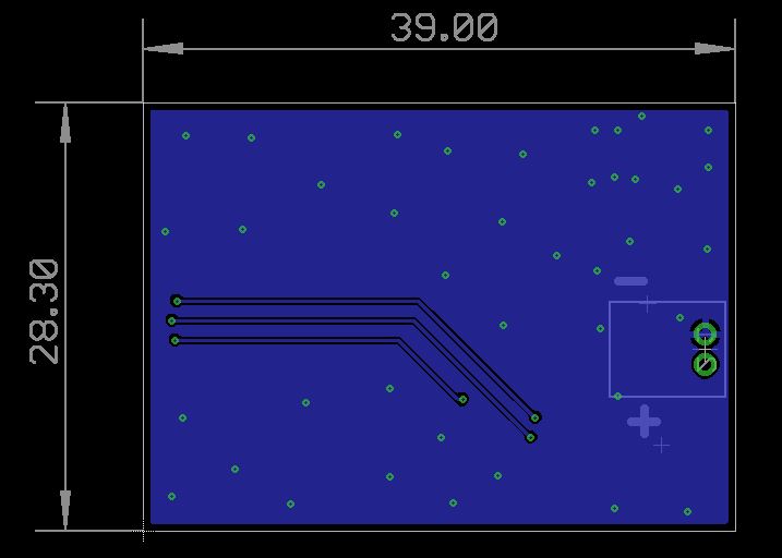
== Layout == | == Layout == | ||
| − | [[File: | + | [[File:Top view.JPG]] |
[[File:Bottom_view_MM002.JPG]] | [[File:Bottom_view_MM002.JPG]] | ||
Latest revision as of 13:04, 14 September 2018
Purpose of this Application Note is to help engineer to integrate MM002 Hardware. This Application Note is valid for all MM002-xx-EU Modules.
Contents
1 Pins assignment
| PAD number | Function | Comment |
|---|---|---|
| 1 | GND | |
| 2 | /NRST | Reset of module. Active at low level. Put a 100nF on this pin. |
| 3 | I2C_SDA / GPIO | I2C bus |
| 4 | I2C_SCL / GPIO | I2C bus |
| 5 | NC | |
| 6 | USART1_RX / GPIO | USART1 |
| 7 | USART1_TX / GPIO | USART1 |
| 8 | NJTRST / GPIO | JTAG Reset |
| 9 | JTDO / GPIO | JTAG Data Output |
| 10 | JTDI / GPIO | JTAG Data Input |
| 11 | JTCK-SWCLK / GPIO | JTAG Clock |
| 12 | JTMS-SWDAT / GPIO | JTAG Mode Select |
| 13 | GPIO | |
| 14 | GPIO | |
| 15 | GND | |
| 16 | GND | |
| 17 | ANT | RF antenna port matched to 50Ω. No DC capacitor required |
| 18 | GND | |
| 19 | SPI_MOSI | SPI bus |
| 20 | SPI_SCK | SPI bus |
| 21 | SPI_MISO | SPI bus |
| 22 | SPI_NSS | SPI bus |
| 23 | USART2_RX / ADC / GPIO | |
| 24 | USART2_TX / ADC / GPIO | |
| 25 | USART2_CTS / WAKEUP1 / ADC / GPIO | |
| 26 | USART2_RTS / ADC / GPIO | |
| 27 | VCC | 3V supply of the board |
| 28 | GND |
2 Application circuit
2.1 Using with companion MCU chipset
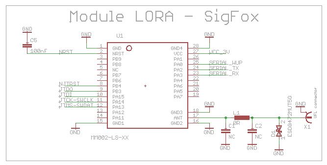
When the module is planned to be controlled with external microcontroller chipset, then the UART connection will be used.
The mandatory module pins to connect to external companion MCU are:
- UART_TX : module pin 24
- UART_RX: module pin 23
- Wake up: module pin 25
Optional pin to connect to companion MCU is RESET (module pin 2). Reset is active at low level.
It is recommended to add a 100nF capacitor on Reset pin: this will avoid any untimely reset of the product due to ESD discharges.
The others I/O pins can be left not connected.
2.2 Power supply
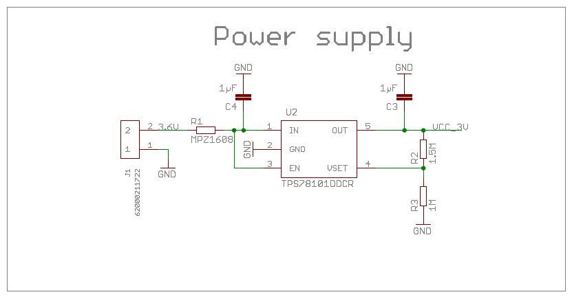
To supply the module, connect to VCC pin 27.
- Recommended
- 3V level with a minimum of 2.7V and maximum of 3.3V.
Internal decoupling capacitors on power supply line inside the module are already placed with capacitors values of 4.7µF and 100nF.
No need to add external decoupling capacitor on VCC pin 27.
We recommend to place a ferrite bead on VCC line: recommended reference is MPZ1608D101B from TDK.
- Impact of power supply level on TX power
The TX power is sensitive to external power level on Vcc.
Measure of TX power level depending of voltage level, and current consumption associated:
   VCC=3.3V: Measure of Tx power on antenna pin=14.2dBm, I=43.5mA
   VCC=3V: Measure of Tx power on antenna pin=13.65dBm, I=40.1mA
   VCC=2.7V: Measure of Tx power on antenna pin=12.85dBm, I=36.6mA
   VCC=2.4V: Measure of Tx power on antenna pin=11.83dBm, I=32.3mA (absolute low voltage level)
   VCC=1.8V: Measure of Tx power on antenna pin=7.73dBm, I=24.5mA (not recommended)
2.3 Antenna connection
On antenna RF pin 17, we recommend to place a pi matching network in order to match the impedance presented by the antenna connected to the board and the impedance presented by module antenna output.
The module antenna output is already matched to 50ohms in the frequency region band chosen.
ESD protection can be added to antenna port if the antenna is external to the product case. We recommend to use ESD8472MUT5G from On Semiconductor.
3 Module PCB
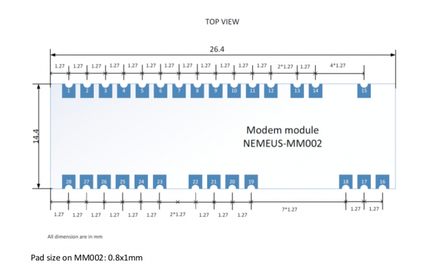
3.1 MM002 module dimensions
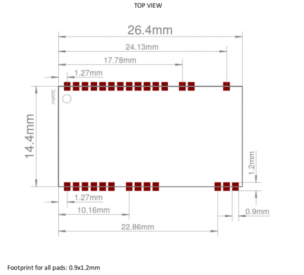
3.2 Layout footprint for MM002 module integration
4 Reference schematic
4.1 BOM of the reference
- TPS78101DDCR from Texas Instrument
- ESD8472MUT5G from On Semiconductors
- ESHF-105-01-L-D-SM from SAMTEC
- UFL connector: U.FL-R-SMT-1(10) from Hirose
- Battery connector: 62000211722 from Wurth Elektronik
4.2 Schematic
In option:
